
I believe that when designing PCBs, everyone will recognize the indispensable step of routing. The rationality of routing not only determines the aesthetics of the PCB and the level of production costs but also reflects the quality of circuit performance, heat dissipation, and whether component performance can be optimized.
This article will provide a comprehensive summary of PCB routing methods.
-
The length of traces should include the lengths of vias and component pads.
-
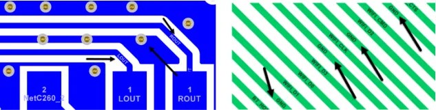
The preferred routing angle is 135 degrees. Any other angle may lead to manufacturing issues during PCB production.

- Avoid routing at right or acute angles, which can cause changes in line width and impedance at corners, resulting in signal reflection, as shown in the figure below.
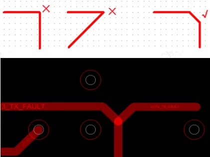
- Routes should exit from the long side of the pad, avoiding exits from the wide side or corners. The corner of the route should be at least 6mil away from the pad, as shown in the figure below.
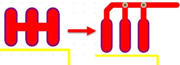
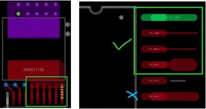
- As shown in the figure below, adjacent pads on the same net should not be directly connected. They should be connected after exiting the pads. Direct connection can easily lead to solder bridging during manual soldering.
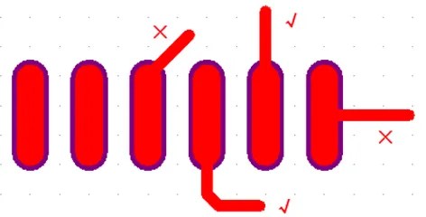
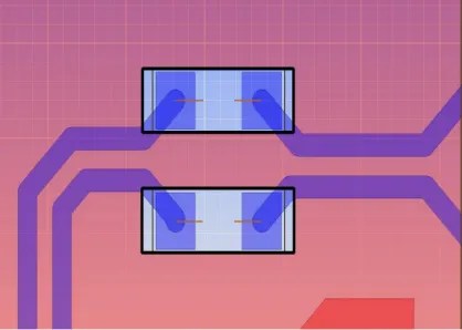
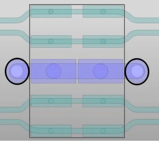
- For small CHIP components, pay attention to the symmetry of routing, maintaining consistent line widths on both ends. If one pin has copper cladding, the other pin should also be copper-clad to reduce component drift and rotation after placement, as shown in the figure below.
- For signals requiring grounding shielding, ensure the integrity of the shielding and try to place GND vias on the shielding traces. The spacing between two GND vias should not be too far, preferably around 50-150mil, as shown in the figure below.
- Traces should have a complete and continuous reference plane to avoid high-speed signals crossing regions. It is recommended that high-speed signals be at least 40mil away from the edge of the reference plane, as shown in the figure below.
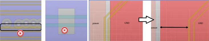
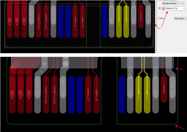
- Since surface-mount component pads can cause impedance reduction, to minimize the impact of impedance changes, it is recommended to remove a layer of the reference plane directly below the pads, matching the size of the pads. Common surface-mount components include capacitors, ESD devices, common-mode choke inductors, connectors, etc., as shown in the figure below.
- As shown in the figure below, the loop area formed by a signal line and its return path should be as small as possible to minimize both external radiation and susceptibility to external interference.
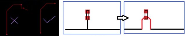
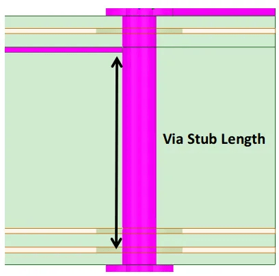
- As shown in the figure (top), stubs in routing are not allowed. Try to minimize stub lengths, preferably to zero. Avoid via stub effects, especially when stub lengths exceed 12mil. In such cases, it is recommended to use simulations to assess the impact of via stubs on signal integrity, as shown in the figure (bottom).
- Avoid forming self-loops with traces on different layers. This issue often arises in multilayer board design and can cause radiation interference, as shown in the figure below.
-
It is recommended not to place test points on high-speed signals.
-
For interfering or sensitive signals (such as RF signals), a shielding canopy should be planned. The conventional width of the shielding canopy is 40mil (preferably 30mil or more, subject to confirmation with the manufacturing vendor). Place as many GND vias on the shielding canopy as possible to enhance its soldering effect.
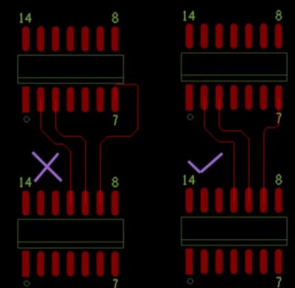
- The trace width should be consistent for the same net. Changes in line width can cause uneven characteristic impedance of the circuit, leading to reflections at higher transmission speeds. Under certain conditions, such as with connector lead-outs or BGA package lead-outs, due to small spacing, changes in line width may be unavoidable. In such cases, minimize the effective length of the inconsistent middle section, as shown in the figure below.

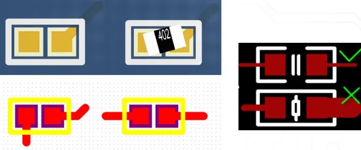
- The line width of IC pin exits should be less than or equal to the pad width. The exit width cannot be wider than the pad width. For some signals with high current carrying requirements and wider line widths, routing can initially match the pin width and then increase the line width about 6-10mil after exiting the pad, as shown in the figure below.
-
Routing must connect to the center of pads and vias.
-
For high-voltage signals, ensure sufficient creepage distance.
-
If the design includes multiple DDR or other memory chips, confirm the routing topology with the customer and verify if there are reference documents.
-
The gold finger area requires a full window opening. In multilayer board design, copper on all layers below the gold fingers should be removed, with a distance of at least 3mm from the board edge.
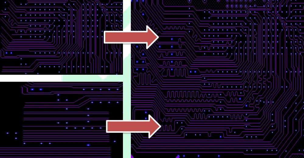
- Plan the routing channels in bottleneck areas ahead of time and reasonably estimate the routing capacity in the narrowest parts of the channels.
-
Coupling capacitors should be placed as close to connectors as possible.
-
Series resistors should be placed close to the transmitting device, and termination resistors should be placed near the end, such as the series resistor on the eMMC clock signal, which is recommended to be placed within 400mil of the CPU side.
-
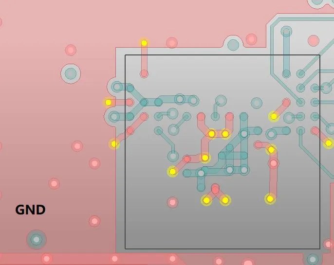
It is recommended to place one GND via on each ground pad of ICs (such as eMMC particles, FLASH particles, etc.) to effectively shorten the return path, as shown in the figure below.
- It is recommended to place one GND via on each ground pad of ESD devices, with the via as close to the pad as possible, as shown in the figure below.
-
Avoid routing near clock components (such as crystals, oscillators, clock generators, clock distributors), switching power supplies, magnetic components, and plated-through holes for connectors.
-
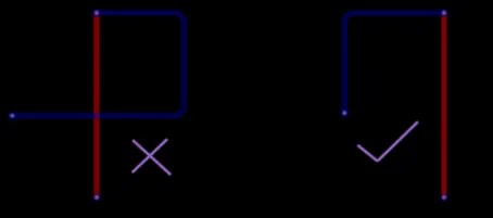
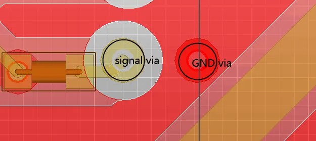
When changing trace layers and the reference planes before and after the change are ground planes, place a companion via next to the signal via to ensure the continuity of the return path. For differential signals, signal vias and return vias should be placed symmetrically, as shown in the figure (top) below. For single-ended signals, it is recommended to place a return via next to the signal via to reduce crosstalk between vias, as shown in the figure (bottom) below.

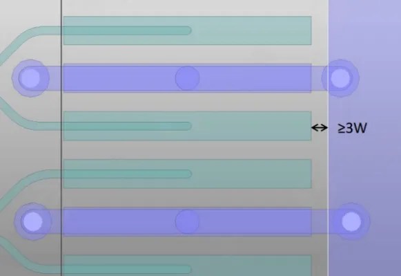
- The distance between the ground copper of connectors and signal pads should be at least 3 times the line width, as shown in the figure below.
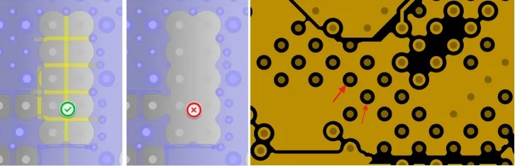
- Connect traces at the planarity discontinuity in the BGA area or perform pad shaving to avoid damaging plane integrity, as shown in the figure below.
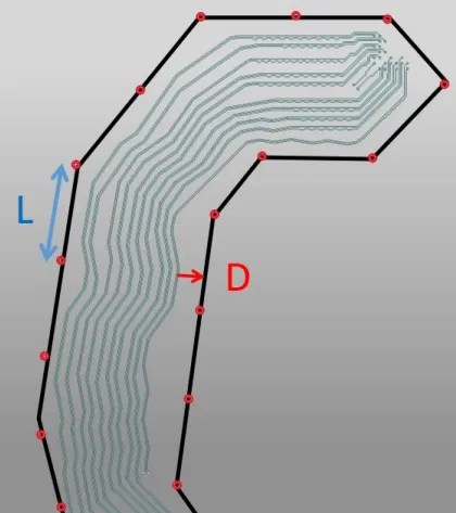
- When PCB routing requires grounding shielding, the recommended shielding method is shown in the figure below, where L is the spacing between grounding vias, and D is the distance between the grounding shield and signal lines, recommended to be ≥4*W.
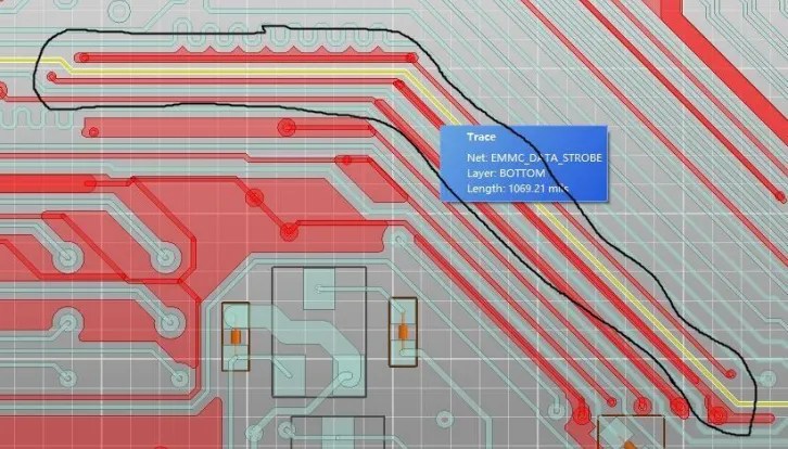
- Some important high-speed single-ended signals, such as clock signals, reset signals, etc. (e.g., emmc_clk, emmc_datastrobe, RGMII_CLK, etc.), should be shielded. Place at least one grounding via every 500mil along the shielding trace, as shown in the figure below.

